
Thin Film & Optical Coating Measurement
Featured Articles
Solar Cell Thin Film Thickness Measurement
Accurate thin film measurement is essential in solar and photovoltaic manufacturing to maximize energy conversion, coating performance, and production quality. Thin photovoltaic layers, transparent conductive oxides, and anti-reflective coatings directly influence solar cell efficiency and long-term device reliability.
Display Thin Film Measurement Applications
Accurate display technology measurement is essential for developing high-performance displays with exceptional brightness, color accuracy, transparency, and long-term reliability. Thin conductive, optical, and protective films directly influence display performance across OLED, LCD, MicroLED, and other advanced display technologies.
Advanced Photonics Thin Film Measurement Applications
Advanced photonic devices require precise optical characterization to optimize light propagation, reduce losses, and improve device performance. Optical coatings, waveguides, photonic integrated circuits (PICs), and laser components all depend on accurate measurement to support development and manufacturing.
Customer Research & Publications
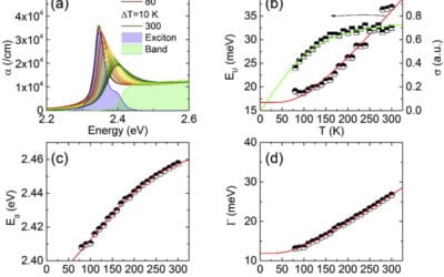
Exciton and lattice dynamics in low-temperature processable CsPbBr3 thin-films
C Wolf, TW Lee - Materials Today Energy, 2017 Abstract Lead-halide based perovskite semiconductors have recently attracted significant attention owing to their rapidly increasing efficiency in solar...
Growth and characterization of GaN/AlGaN heterostructures on GaN substrate templates
L Hubbard, N Dietz, M Vernon, R Collazo, S Mita… - … International Conference on …, 2017 This contribution will present the structural and optoelectronic properties of GaN/AlGaN heterostructures...
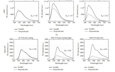
Polarized Emission from Conjugated Polymer Chains Aligned by Epitaxial Growth during Off-Center Spin-Coating
T Anzai, W Porzio, V Vohraa Due to their macromolecular nature, conjugated polymers can be relatively easily aligned by applying a variety of processes resulting in either elongation or ordering of...
ZnO film deposition by DC magnetron sputtering: Effect of target configuration on the film properties
E Arakelova, A Khachatryan, A Kteyan, K Avjyan… - Thin Solid Films, 2016 Ballistic transport model for target-to-substrate atom transfer during magnetron sputter deposition was used to develop zinc...
Influence of doping behavior of Al on nanostructure, morphology and optoelectronic properties of Al Doped ZnO thin film grown on FTO substrate
M Shirazi, RS Dariani, MR Toroghinejad - Journal of Materials Science Al doped ZnO nanostructures deposited on FTO glass substrate by spray pyrolysis method with different Al doping levels...
Formation mechanism of toxic-element-free oxide layer on Ti–6Al–4V alloy in d.c. glow discharge plasma with pure oxygen gas
K Satoh, S Sato, K Wagatsuma - Surface and Coatings Technology, 2016 The purpose of this study is to elucidate the formation mechanism of a toxic-element-free oxide layer on a Ti–6Al–4V alloy by...
Spectroscopy Applications
Food Safety & Quality
Advanced & quantum materials
Astronomy, Space & Remote Sensing
Pharmaceuticals & Nutraceuticals
Biomedical & Life Sciences
Environmental & Microplastics
Industrial & Process Analysis
Lighting, Displays & Radiometry
Recommended Thin Film Measurement Systems
Learn More
Explore thin film metrology through practical guides, application notes, videos, technical resources, and real-world research. From understanding thin film thickness measurement to exploring optical coatings, reflectance and transmission, and advanced materials, the Thin Film Learning Center provides resources to help you better understand measurement techniques and get more from your thin film analysis.
- Guides & Technical Resources — Learn about measurement techniques, optical characterization, and thin film analysis.
- Application Notes & Research — See how thin film metrology is used across semiconductors, solar, displays, coatings, and advanced materials.
- Videos, Software & Tools — Explore demonstrations, software resources, technical documents, and measurement tips.