L Hubbard, N Dietz, M Vernon, R Collazo, S Mita… – … International Conference on …, 2017
This contribution will present the structural and optoelectronic properties of GaN/AlGaN heterostructures grown by Metal Organic Chemical Vapor Deposition (MOCVD) on GaN/sapphire templates. The target parameters for the materials heterostructures have been modeled for utilization in Avalanche Photodiode Detector Structures (APD) operating in the near and deep UV region. Optical modeling has improved absorption within the heterojunction as well as maximized light trapping within the device. Electronic modeling has determined the optimal dopant concentrations for maximum impact ionization rate, as well as tolerance to defects and unintentional doping. This application will require advances in the defect densities, surface morphology, and interfaces. Surface morphological and structural properties of GaN/AlGaN heterostructures are analyzed by Atomic Force Microscopy, Raman spectroscopy, and X-ray diffraction. The optoelectronic properties (phonon structures, free carrier concentrations, and carrier mobility) as well as layer thickness information, are determined by Fourier Transform Infrared Reflectance spectroscopy. A correlation of interfacial defects (type and concentration) with microscopic structural properties, surface morphology, and optoelectronic properties (free carrier concentration and high-frequency dielectric function) is discussed.
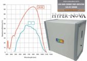
… Spectral NI reflectance spectroscopic measurements were carried out from 200 nm to 1100nm using a Deuterium/Halogen light source, a StellarNet SILVER- Nova spectrometer with a TE-cooled linear CCD array, and associated corrective optics. …