Thin Film Metrology
Looking for a thin film measurement solution? StellarNet Thin Film Metrology Systems provide fast, non-contact characterization of thin films and coatings for research, manufacturing, and quality control applications. Explore configurable solutions for thin film thickness measurement, optical coating analysis, semiconductor processes, and advanced materials research.
Thin film metrology is essential for the development and manufacturing of modern optical coatings, semiconductor devices, displays, photovoltaic materials, and advanced engineered surfaces. Accurate characterization of film thickness, optical properties, and coating uniformity helps ensure product performance, process consistency, and manufacturing yield.
StellarNet Thin Film Metrology Systems combine advanced optical spectroscopy and spectroscopic reflectometry techniques with high-performance spectrometers, optical accessories, and powerful analysis software to measure thin films and coatings. These flexible platforms support optical coating characterization, semiconductor metrology, process monitoring, and advanced materials research across research, manufacturing, and quality control environments.
Thin Film Measurement Techniques
Learn the non-contact optical techniques used to measure thin film thickness, optical properties, and multilayer structures.
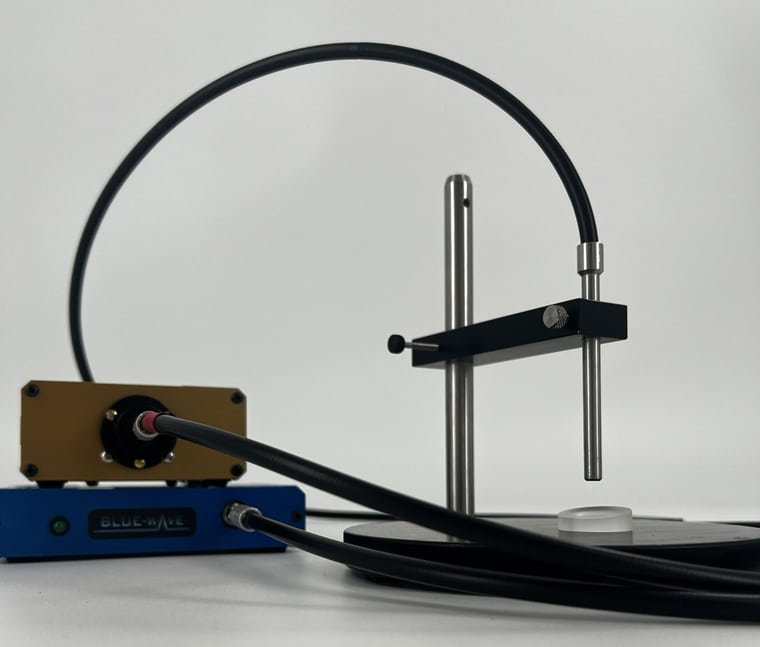
Thin Film Thickness Measurement
Measure thin film and coating thickness using non-contact optical spectroscopy techniques. Ideal for optical coatings, semiconductor devices, displays, and advanced materials research
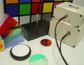
Reflectance & Transmission Spectroscopy
Determine thin film thickness and optical properties through analysis of reflected light. Provides fast, accurate measurements for coating characterization and process monitoring.
Industry Applications
Discover how Thin Film Measurement Systems support research, manufacturing, and quality control across a wide range of industries.
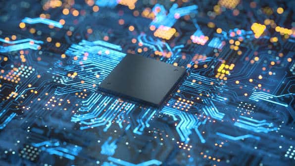
Semiconductor Metrology
Measure thin films, dielectric layers, photoresists, and deposited coatings used in semiconductor manufacturing. Supports wafer characterization, process monitoring, and quality control.
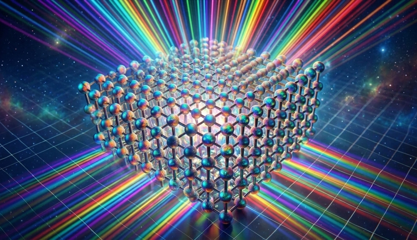
Photonic Device Measurement
Characterize silicon photonics, PICs, optical waveguides, laser optics, and quantum photonic devices using non-contact thin film metrology and optical characterization.
Solar & Photovoltaic Measurement
Analyze thin film solar cells, photovoltaic coatings, and energy materials using optical spectroscopy. Supports research, development, and production quality verification.
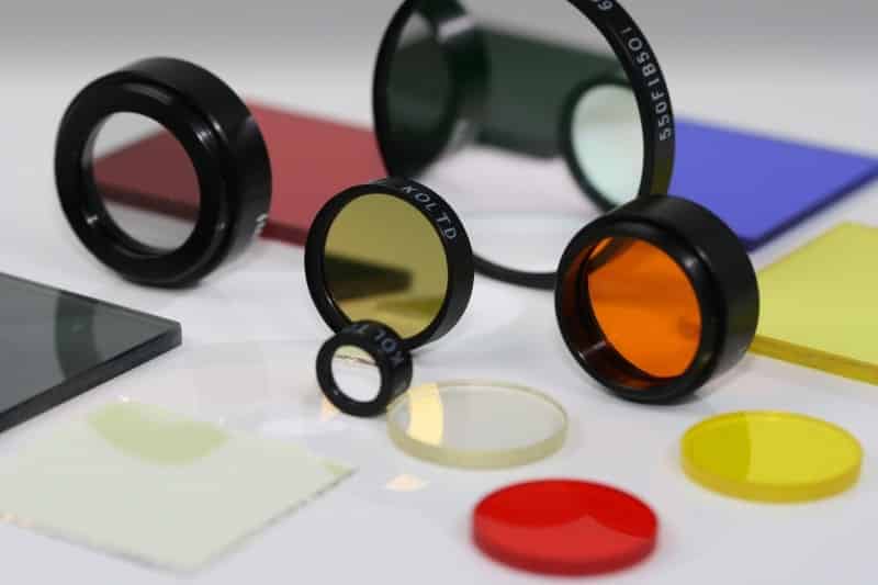
Optical Coating Measurement
Characterize anti-reflective coatings, optical filters, mirrors, and laser optics. Verify coating thickness, uniformity, and optical performance with spectroscopic metrology techniques.
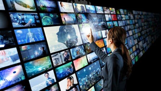
Display Technology Measurement
Characterize thin films and coatings used in LCD, OLED, and MicroLED displays. Supports process development, quality assurance, and display performance evaluation.
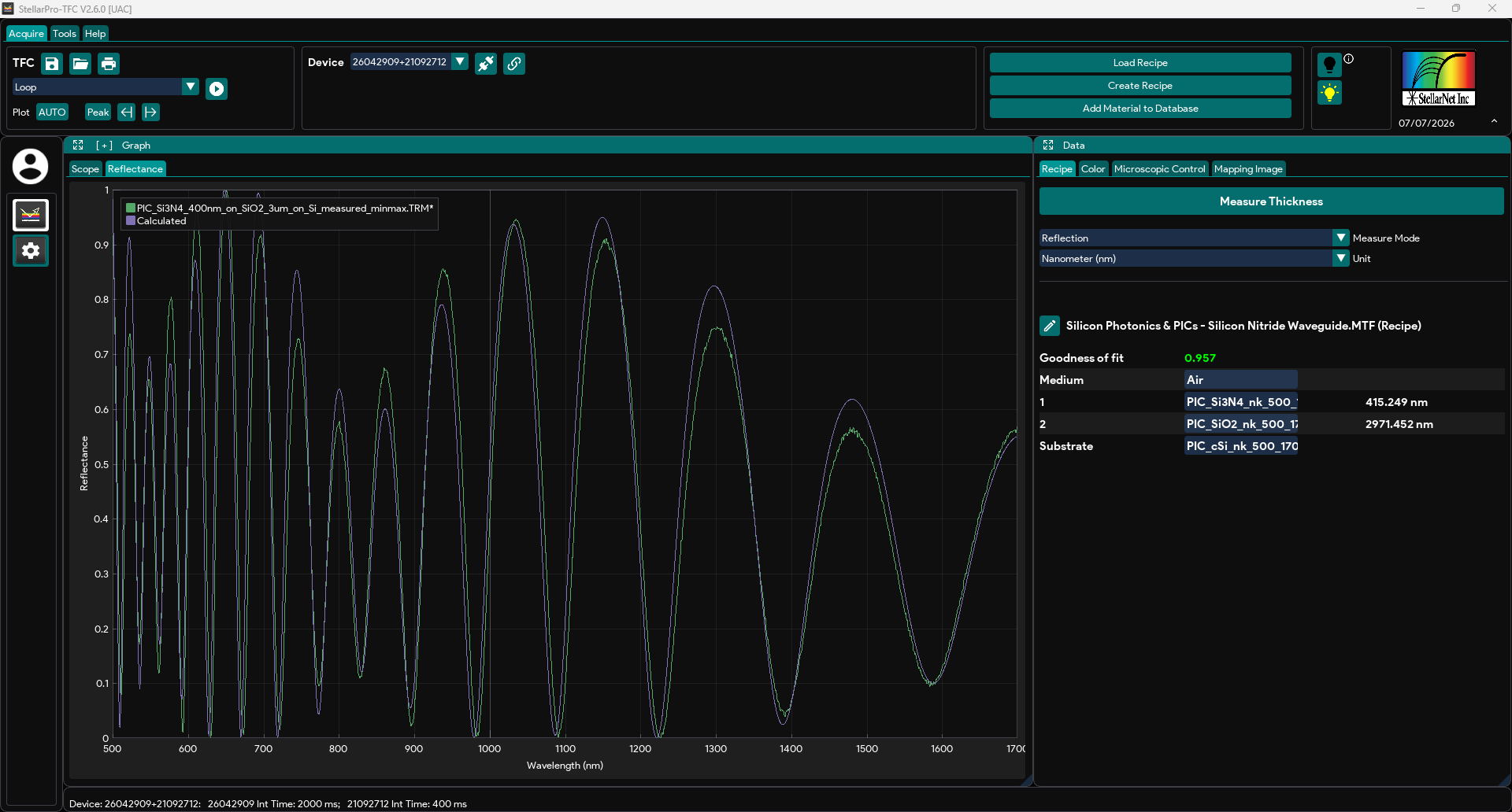
Featured Application: Silicon Nitride Waveguide Measurement
Silicon nitride (Si₃N₄) waveguides are fundamental building blocks for silicon photonics, photonic integrated circuits (PICs), optical communications, LiDAR, and emerging quantum photonic devices. Precise control of waveguide and dielectric layer thickness is essential for achieving accurate optical confinement, wavelength response, and low propagation loss. A StellarNet Thin Film Measurement System provides rapid, non-contact characterization of multilayer waveguide structures using optical reflectance spectroscopy, supporting research, process development, and production quality control.
Typical Measured Stack
Air
Silicon Nitride (Si₃N₄) (~350 nm)
Silicon Dioxide (SiO₂) (~2–3 µm)
Silicon Substrate
Recommended Thin Film System: 400–1700 nm (TF-VIS-NIR)
Frequently Asked Questions About Thin Film Metrology
What is thin film metrology?
Thin film metrology is the science of measuring and characterizing thin films, coatings, and deposited layers. Common measurements include film thickness, optical properties, coating uniformity, reflectance, and transmission characteristics.
What types of thin films can be measured?
Thin film metrology systems are commonly used to evaluate optical coatings, dielectric layers, semiconductor films, photoresists, solar cell materials, display coatings, and advanced engineered surfaces used in research and manufacturing.
What is the difference between thin film metrology and film thickness measurement?
Film thickness measurement focuses on determining the thickness of a coating or deposited layer. Thin film metrology encompasses a broader range of measurements including thickness, optical properties, refractive index, reflectance, transmission, and coating performance.
What measurement techniques are used in thin film metrology?
Common techniques include spectroscopic reflectometry, reflectance spectroscopy, transmission spectroscopy, ellipsometry, and interferometry. The optimal technique depends on the material, thickness range, substrate, and measurement requirements.
Why use optical spectroscopy for thin film measurements?
Optical spectroscopy provides rapid, non-contact, and non-destructive measurements while supporting a wide range of materials and thickness ranges. Spectroscopic techniques can often evaluate both film thickness and optical properties from a single measurement.
How are StellarNet thin film metrology systems different from traditional dedicated metrology instruments?
StellarNet systems combine thin film measurement capabilities with the flexibility of modular spectroscopy platforms. This allows users to support research, process development, quality control, optical characterization, and multiple measurement applications using a common hardware and software architecture.
Can a thin film metrology system perform measurements beyond film thickness?
Yes. Depending on the configuration, systems can be used for reflectance measurements, transmission measurements, optical coating characterization, material analysis, semiconductor process monitoring, and other spectroscopy-based measurements.
Are StellarNet thin film metrology systems suitable for both research and manufacturing?
Yes. StellarNet solutions are used in research laboratories, universities, production facilities, and OEM environments. Their modular architecture allows systems to be configured for both development work and routine quality control applications.
What industries use thin film metrology systems?
Thin film metrology is widely used in semiconductor manufacturing, photonics, optical coating production, display technologies, solar energy, advanced materials research, aerospace, and precision manufacturing.
Can thin film metrology systems be customized for specific applications?
Yes. Measurement systems can be configured with different spectrometers, wavelength ranges, optical accessories, sampling geometries, and software tools to address specific application requirements.
What are the advantages of spectroscopic thin film metrology?
Spectroscopic techniques provide fast measurements, non-contact operation, minimal sample preparation, excellent repeatability, and the ability to characterize multiple film properties from a single analysis.
How do I choose the right thin film metrology system?
The best system depends on the material being measured, thickness range, substrate type, measurement speed, required accuracy, and application goals. Factors such as reflectance, transmission, coating characterization, semiconductor measurements, and future expansion requirements should also be considered.
How should I cite a StellarNet spectrometer in my research?
Check out our guide on citing instrumentation in your research: https://www.stellarnet.us/how-to-cite-a-spectrometer/
Thin Film Metrology Applications Overview
Semiconductors
Our systems can measure thickness of non-metallic semiconductor process films. Also, these Thin Film Measurement systems can be used to locate and identify the cause of failure in integrated circuits. Systems are also used during MEMS patterning processes to measure photoresist thickness and uniformity. These systems are also being used during silicon etching to measure etch rate and membrane thickness and uniformity. Thickness measurement of thick polysilicon films and SOI are also common applications.
Polymer Films
Polymer films such as PET and polycarbonate require monitoring of film thickness during manufacturing. 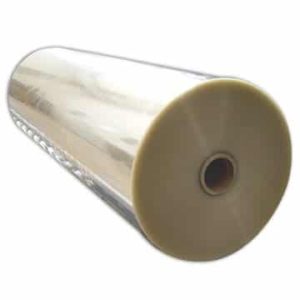
Optics
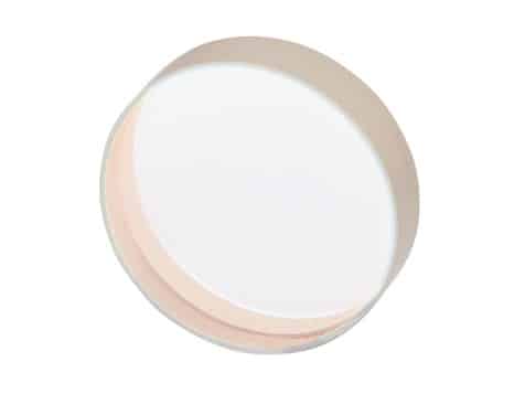 Optical coatings are used to enhance the reflectance and transmittance properties of a substrate material. StellarNet Thin-Film Measurement systems can be used to measure anti-reflection, increased reflection coatings, high-pass, low-pass, and bandpass filters. StellarNet spectrometer systems also come with StellarPro Software for CIELAB colorimetry. See our colorimeter page.
Parylene Coatings
Parylene Coatings
Parylene and a variety of poly (p-xylylene) polymers are used extensively as moisture barriers and electrical insulators and their coating thicknesses can be measured via reflectance spectroscopy. Parylene applications included coatings for printed circuit boards and medical devices such as stents and pacemakers, permanently implanted in the body.
Thick Resists
Thick Resists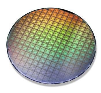
Thick photoresists such as SU-8, a commonly used epoxy based negative photoresist normally spun in layers from 0.1um to 2mm. Monitoring of thickness can be crucial during production and fabrication of multilayer stacks.
Displays
Most flat panel displays including LCD, OLED, and many other display technologies employ transparent conductive oxides (TCOs) to 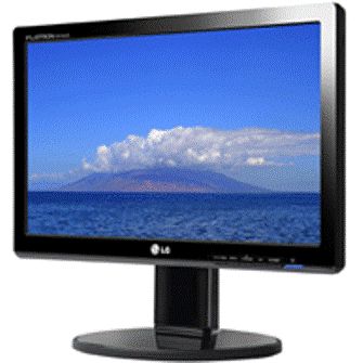 transport current to each light-emitting element of the display. Thin Film Measurement Systems can be used to measure the thickness of Liquid Crystal layers such as polyamide, hardcoat, and air gap. For OLED displays, systems are able to measure layers such as emissive, injection, buffer, and the encapsulation layer.
Ophthalmic Lens Coatings
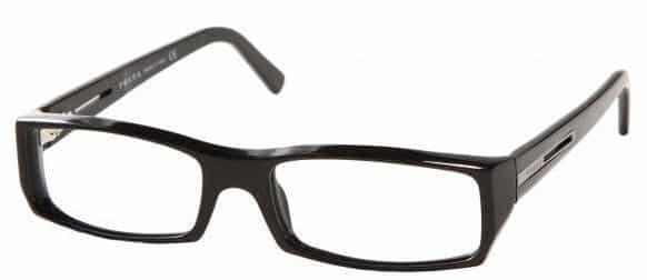 StellarNet Thin-Film Measurement Systems can be used to measure coatings on Ophthalmic Lenses. Spectral reflectance can be used to measure anti-reflectance coatings on lenses as well as hardcoat and hydrophobic layer thickness.
Hardcoat Measurements
Hardcoat Measurements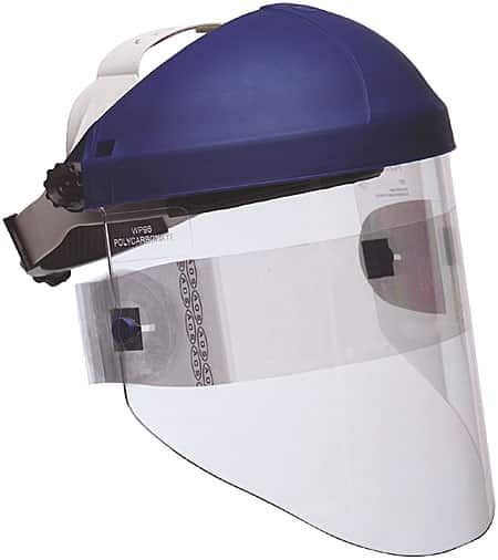
Many industries use hardcoats and various protective coatings. Layer thickness and thickness monitoring is extremely important for manufacturing and quality control.ion.
Vacuum Deposition
Vacuum Deposition
Vacuum deposition is a family of processes used to deposit layers atom-by-atom or molecule-by-molecule at sub-atmospheric pressure on a solid surface. The layers may be as thin as one atom to millimeters thick (freestanding structures). There may be multiple layers of different materials (e.g. optical coatings). A thickness of less than one micrometer is generally called a thin film while a thickness greater than one micrometer is called a coating. StellarNet Thin-Film measurement systems can be used to check the deposition thickness of a wide range of materials.
n.
Why Customers Choose StellarNet
- Engineer-owned and operated
- Flexible thin film metrology solutions, not one-size-fits-all systems
- Non-contact optical measurement technologies
- Reflectance and transmission spectroscopy expertise
- Modular hardware for evolving measurement requirements
- UV, VIS, NIR, and Raman wavelength coverage
- Rapid customization and OEM integration capabilities
- Research-to-production scalability
- Cross-platform software and analysis tools
- US-based engineering and application support
Thin Film Measurement Demo Video

Find the Right Thin Film Metrology Solution
From thin film thickness measurement and optical coating characterization to semiconductor process monitoring and advanced materials research, StellarNet provides flexible thin film metrology solutions for laboratory and manufacturing environments. Compare measurement techniques and application-specific solutions to find the best approach for your film characterization requirements.
Search our Film Metrology Knowledge Base
Popular Topics Include :
Thin Film • Solar • Optical • Display
Film Metrology Learning Center
Check out all of our film measurement manuals, technical specification, drawings, communication protocols, SDK info and much more!
Film Measurement Customer Applications
Technical Information Request

Application Note: Cyclospora Food Saftey
The 2026 Cyclospora outbreak linked to iceberg lettuce highlights a persistent challenge in food production: contamination can move through the supply chain before conventional testing identifies a problem. Emerging research suggests that NIR, Raman/SERS, chemometrics...