
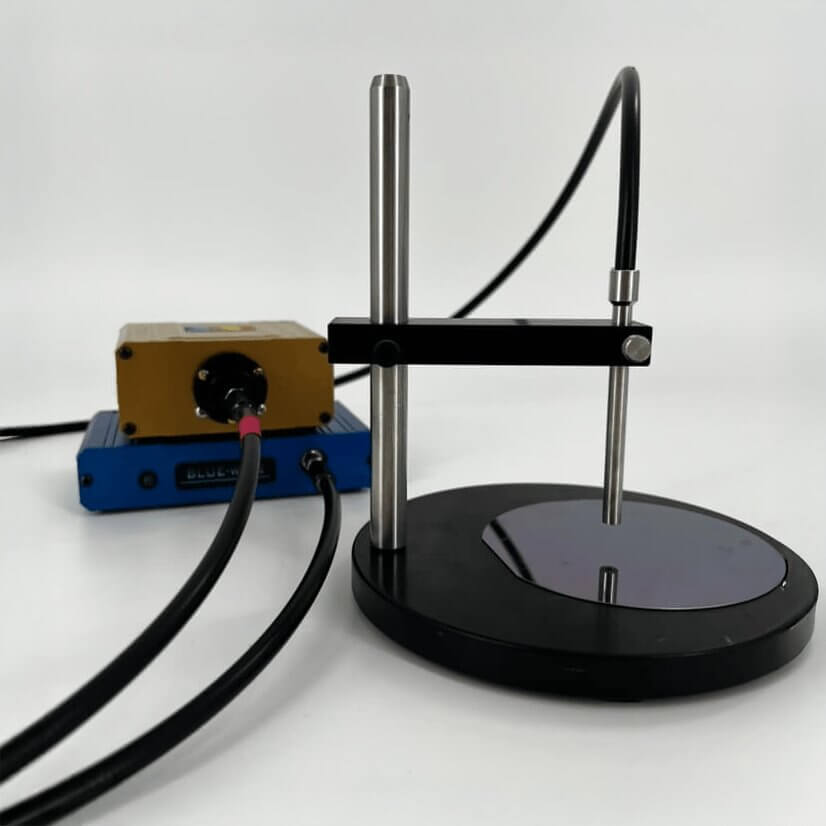
Semiconductor Measurement
Need a semiconductor measurement solution for your application? Our configurable thin film metrology systems deliver rapid, non-contact optical measurements for process development, wafer characterization, quality assurance, and manufacturing consistency. Speak with our team to configure a system tailored to your measurement requirements.
StellarNet systems combine reflectance and transmission spectroscopy with modular optical measurement platforms to characterize semiconductor materials, including thin films, dielectric layers, photoresists, and deposited coatings. Designed for both research laboratories and production environments, these flexible systems support semiconductor process monitoring, thin film characterization, and advanced materials development while adapting to evolving manufacturing requirements.
Common Semiconductor Thin Films
- Silicon Dioxide (SiO₂) – Gate Oxides & Insulation
- Silicon Nitride (Si₃N₄) – Passivation & Dielectric Layers
- High-k Dielectric Films – Advanced CMOS Devices
- Low-k Dielectric Films – High-Speed Interconnects
- Polysilicon – Gate Electrodes & Device Structures
- Transparent Conductive Oxides (ITO) – Optoelectronic & Display Devices
- Thin Metal Films – Contacts, Interconnects & Electrodes
- Photoresist Layers – Photolithography & Process Development
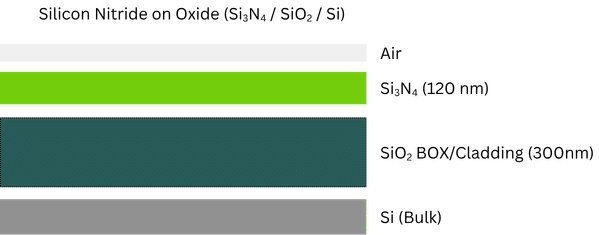
Cross-sectional semiconductor thin film stack showing silicon nitride (Si₃N₄), silicon dioxide (SiO₂), and silicon substrate used for thin film measurement and wafer characterization.
Key Semiconductor Film Measurements
Accurate semiconductor measurement requires more than determining thin film thickness alone. Engineers evaluate multiple optical and material properties to monitor fabrication processes, verify layer integrity, improve device performance, and maintain manufacturing consistency.
Typical semiconductor measurements include:
- Thin Film Thickness
- Reflectance
- Transmission
- Layer Uniformity
- Optical Constants (n & k)
- Process Monitoring & Wafer Characterization
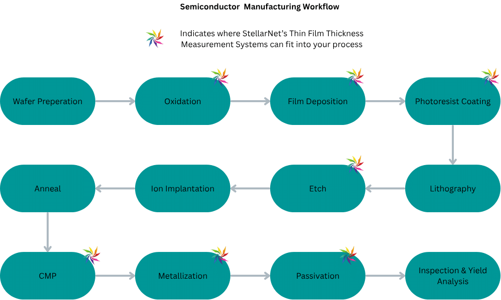
Simplified semiconductor manufacturing workflow showing key fabrication stages where thin film metrology and optical characterization support process monitoring and quality control: Wafer Preparation → Oxidation → Film Deposition → Photoresist Coating → Lithography → Etch → Ion Implantation → Anneal → Chemical Mechanical Planarization (CMP) → Metallization → Passivation → Inspection & Yield Analysis.
Applications for Semiconductor Measurement
Silicon Nitride on Oxide (Si₃N₄ / SiO₂ / Si)
Silicon nitride (Si₃N₄) deposited on thermal oxide is commonly used for passivation, stress engineering, masking, diffusion barriers, and MEMS fabrication. Simultaneous measurement of silicon nitride and underlying oxide thickness enables accurate multilayer process control throughout semiconductor production. Using Transfer Matrix Method (TMM) modeling, multilayer dielectric stacks can be characterized quickly and nondestructively for improved manufacturing consistency and yield.
Typical Recipe
- Air
- Si₃N₄ (120 nm)
- SiO₂ BOX/Cladding (300 nm)
- Si (Bulk)
Recommended Thin Film System: 350–900nm (TF-UVVIS)
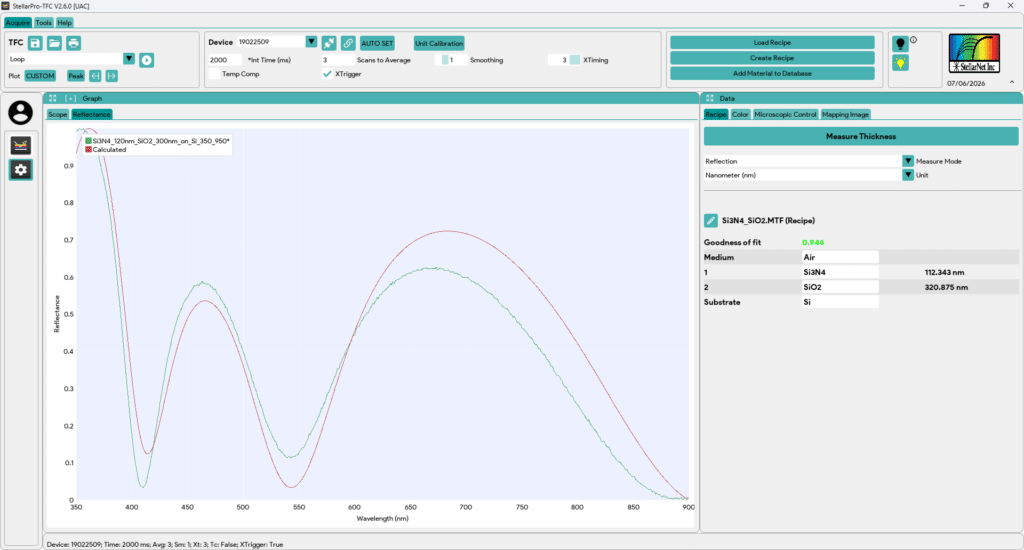
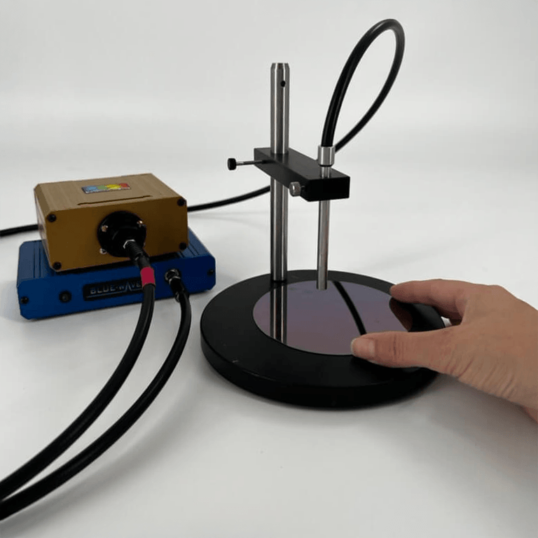
Semiconductor dielectric layer measurement of a silicon nitride on silicon dioxide (Si₃N₄/SiO₂/Si) film stack using a StellarNet Thin Film Measurement System (TF-UVVIS).
Thermal Oxide (SiO₂) Thickness Measurement
Thermal silicon dioxide (SiO₂) is one of the most widely used dielectric materials in semiconductor manufacturing, serving as a gate oxide, isolation layer, masking layer, and surface passivation. Accurate oxide thickness measurement is critical for maintaining electrical performance and process consistency. Spectroscopic reflectometry provides fast, non-contact measurement of thermal oxide films from only a few nanometers to several micrometers with excellent repeatability, making it ideal for wafer process monitoring, quality control, and research applications.
Typical Recipe
- Air
- SiO₂
- Si (Bulk)
Recommended Thin Film System: 350–900 nm (TF-UVVIS)
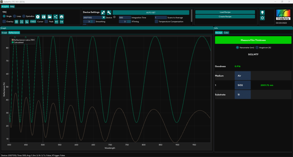
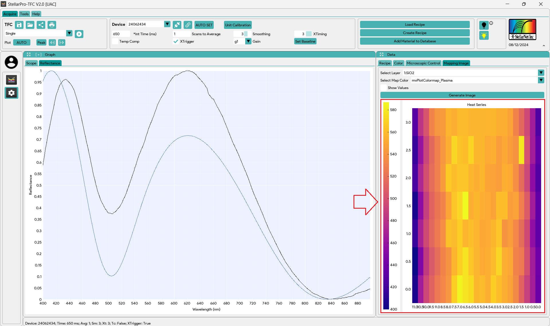
Silicon dioxide (SiO₂) thin film measurement using StellarPro-TFC thin film analysis software and optical reflectance spectroscopy for semiconductor wafer characterization.
Photoresist Thickness Measurement
Photoresist thickness plays a critical role in photolithography, directly affecting exposure, pattern transfer, etching, and device fabrication. Spectroscopic reflectometry provides rapid, non-contact measurement of positive and negative photoresists across a wide range of thicknesses, from thin imaging resists to thick MEMS process resists. This enables reliable process control, spin coating optimization, and production quality assurance while eliminating the need for destructive measurements.
Typical Recipe
- Air
- AZ P4620 Photoresist (12000 nm)
- Si (Bulk)
Recommended Thin Film System: 900–1700 nm (TF-NIR)
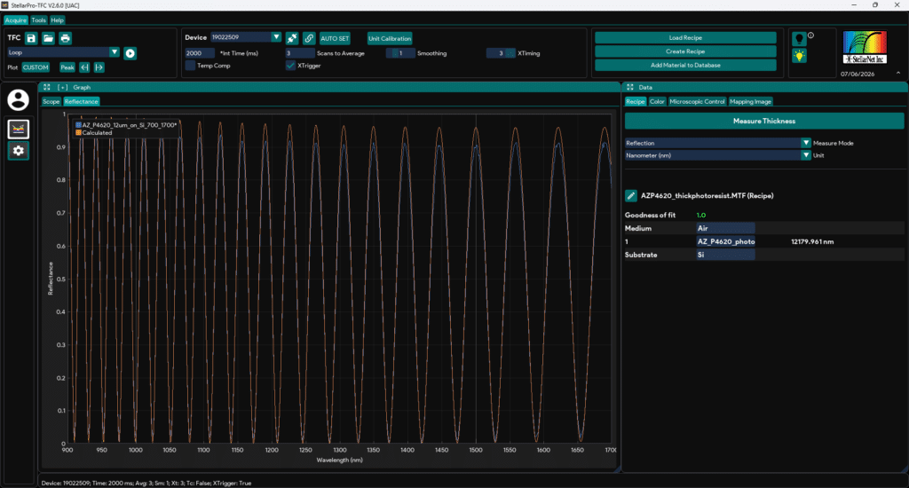
StellarNet Thin Film Measurement System (TF-NIR) measuring thick photoresist film thickness using reflectance spectroscopy for semiconductor process monitoring, wafer characterization, and thin film metrology.
Polysilicon (Poly-Si) Thickness Measurement
Polysilicon thin films are widely used in transistor gates, MEMS structures, sensors, and advanced semiconductor devices. Accurate polysilicon thickness measurement is essential for maintaining device performance and process repeatability. Near-infrared spectroscopic reflectometry provides excellent sensitivity for measuring micron-scale polysilicon films deposited on oxide or silicon substrates, enabling fast, non-contact thickness measurement for wafer inspection, process development, and production monitoring.
StellarNet Recommended Thin Film Metrology Systems for Semiconductor Applications
Every semiconductor application has unique measurement requirements based on film materials, wafer substrates, process stages, and measurement accuracy. StellarNet’s modular thin film metrology platform allows users to configure complete measurement systems using UV-VIS, and NIR spectrometers, reflectance and transmission fixtures, stabilized light sources, fiber optic probes, and advanced thin film analysis software.
From oxide layers and photoresists to dielectric films, transparent conductive oxides, and other semiconductor materials, our flexible systems support research, process development, wafer characterization, and production quality control. Our engineer-owned team works directly with customers to configure reliable, non-contact measurement solutions tailored to their semiconductor applications.
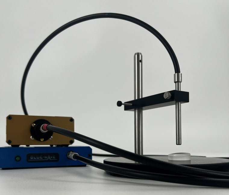
StellarNet TF™ Systems
StellarNet TF™ Systems combine reflectance spectroscopy, precision optics, and intuitive StellarPro™-TFC, Thin-Film Metrology software, to deliver accurate, non-destructive film thickness measurements from approximately 1 nm to 300 µm. The modular architecture allows laboratories to configure the ideal system today while providing a straightforward upgrade path for future automation and advanced measurement capabilities.
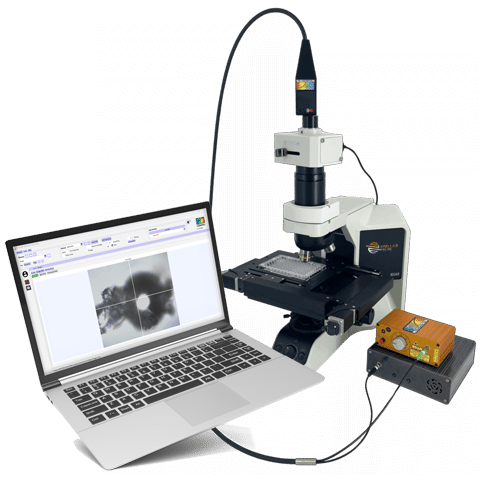
TF-Micro™
TF-Micro™ upgrades any compatible StellarNet TF™ System with a high-resolution microscope, enabling precision thin-film thickness measurements of microscopic features and small sample areas.
TF-Micro-AM
TF-Micro-AM™ adds programmable XY automation to compatible StellarNet TF™ Systems and TF-Micro™, enabling automated thickness mapping, repeatable positioning, and comprehensive measurement documentation for research and process development applications.
Thin Film Measurement Systems
| System | Range (nm) | Resolution | Thickness | Lamp type | Price |
|---|---|---|---|---|---|
TF-VIS | 400-1000 | <2nm | 10nm-75um | Visible/NIR | $11,500 |
| TF-UVVIS | 200-1100 | <2.5nm | 1nm-75um | UV + Visible/NIR | $14,625 |
| TF-NIR | 900-1700 | <5nm | 100nm-300um | Visible/NIR | $22,655 |
| TF-VIS-NIR | 400-1700 | <2nm, 5nm>1000nm | 10nm-300um | Visible/NIR | $25,280 |
| TF-UVVIS-NIR | 200-1700 | <2nm, 5nm>1000nm | 1nm-300um | UV + Visible/NIR | $28,245 |
| TF-Micro | StellarNet configured Microscope equipped with 4,10, & 40x objectives, CMOS 1.3 Mpixel Camera, optical switch, and required coupling accessories | $11,550.00 |
| TF-Micro-AM | StellarNet configured Auto-Mapping Microscope equipped with 4,10, & 40x objectives, CMOS 1.3 Mpixel Camera, optical switch, and required coupling accessories | $30,975.00 |
Thin Film System Specifications
| Precision | 0.1Å or 0.01% (greater of) |
| Accuracy | 0.2% or 10A (greater of) Film stack dependent |
| Stability | 0.2A or 0.02% (greater of) |
| Spot size | 3mm standard, optional down to 3 µm |
| Sample size | Sample size from 1 mm |
| Computer OS | StellarPro-TFC Software designed for 32 and 64-bit OS |
Technical Information Request
BSA Mediated Stabilized Dispersion of Hydrophobic Organic Nanoparticles Produced by Pulsed Laser Fragmentation in Liquid
Akiko Sunada, Tomosumi Kamimura, and Ryohei Yasukuni | Journal of Laser Micro Nanoengineering | August 1, 2026 | 10.2961/jlmn.2026.02.2009 Abstract The complex synthesis of nanopharmaceuticals still faces hurdles regarding stability, sterilization, storage, and...