
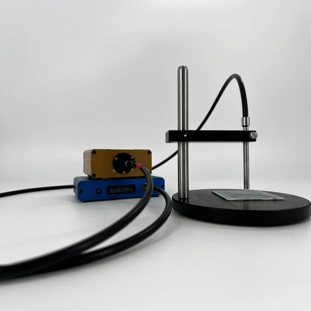
Solar and Photovoltaic Measurement
Looking for a solar or photovoltaic measurement solution? Our configurable thin film metrology systems deliver rapid, non-contact optical measurements for photovoltaic research, process development, manufacturing, quality control, and improved production consistency. Speak with our team to configure a system for your application.
StellarNet Solar & Photovoltaic Measurement Systems combine reflectance and transmission spectroscopy with modular optical measurement platforms to characterize anti-reflective coatings, transparent conductive oxides (TCOs), thin-film solar cells, and other advanced photovoltaic materials. Designed for both research and production environments, these flexible systems support accurate optical characterization to improve device efficiency, long-term performance, and renewable energy innovation.
Common Solar & Photovoltaic Thin Films
- Anti-Reflective (AR) Coatings – Improve Light Transmission
- Transparent Conductive Oxides (ITO, AZO) – Front Electrodes
- Silicon Nitride (SiNx) – Anti-Reflective & Passivation Layers
- Transparent Conductive Films – Solar Cell Electrodes
- Thin Film Photovoltaic Layers – Research & Development
- Perovskite Thin Films – Next-Generation Solar Cells
- CdTe & CIGS Thin Films – Thin Film Photovoltaics
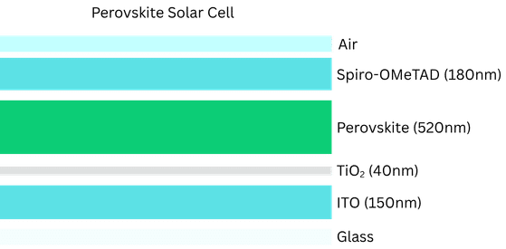
Cross-sectional perovskite solar cell film stack illustrating transparent conductive oxide, electron transport layer, perovskite absorber, hole transport layer, and metal electrode for thin film metrology and photovoltaic characterization.
Key Solar & Photovoltaic Film Measurements
Accurate solar and photovoltaic measurement requires more than determining thin film thickness alone. Engineers evaluate multiple optical and material properties to optimize energy conversion efficiency, verify coating performance, improve device reliability, and maintain manufacturing consistency.
Typical solar and photovoltaic measurements include:
- Thin Film Thickness
- Reflectance
- Transmission
- Optical Absorption
- Layer Uniformity
- Optical Constants (n & k)
- Photovoltaic Characterization & Process Monitoring
Applications for Solar & Photovoltaic Measurement
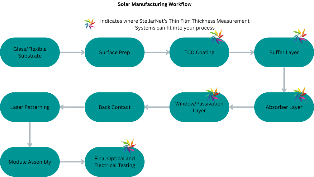
Solar and photovoltaic measurement is essential throughout the development and manufacturing of high-efficiency solar technologies, where thin films and optical coatings directly impact energy conversion and device performance. StellarNet thin film metrology systems support the characterization of photovoltaic coatings, transparent conductive oxides, anti-reflective coatings, thin film solar cells, and advanced energy materials used in research, process development, and manufacturing. By providing rapid, non-contact measurements of film thickness and optical properties, these systems help engineers optimize solar cell efficiency, verify coating consistency, improve production quality, and accelerate the development of next-generation photovoltaic technologies.
Silicon Nitride (SiNx) Anti-Reflection Coating (PERC Solar Cells)
Silicon nitride (SiNx) anti-reflection coatings are one of the most critical thin films used in crystalline silicon PERC solar cells. Besides reducing surface reflection to maximize light absorption, the SiNx layer also provides excellent surface passivation, improving cell efficiency and long-term reliability. Precise control of SiNx thickness directly impacts optical performance and overall power conversion efficiency. Spectroscopic reflectometry provides fast, non-contact measurement of silicon nitride coatings during process development and high-volume production, making it an ideal solution for inline quality control.
Typical Recipe
- Air
- SiNx (75 nm)
- Crystalline Silicon (Bulk)
Recommended Thin Film System: 350–1000 nm (TF-UVVIS)
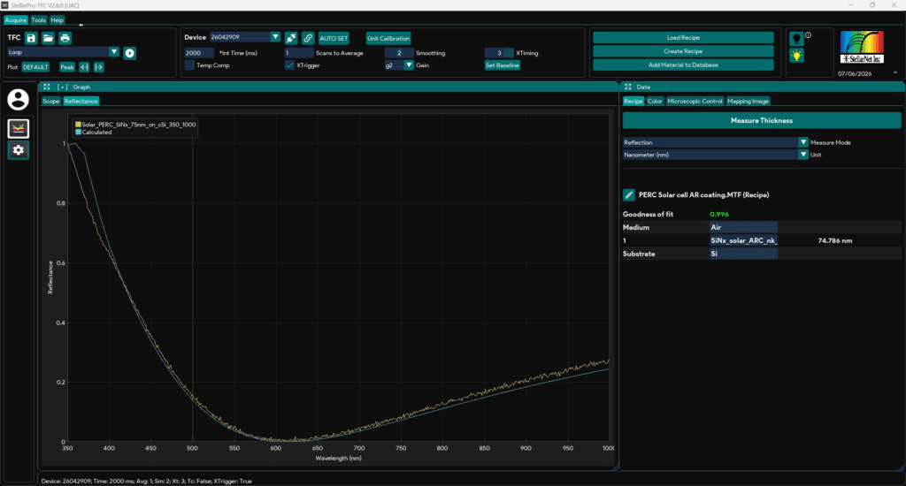
StellarNet Thin Film Measurement System (TF-UVVIS) analyzing a silicon nitride (SiNx) anti-reflection coating on a PERC photovoltaic cell to determine film thickness and optical properties using reflectance spectroscopy.
Transparent Conductive Oxide (ITO) Thickness Measurement
Indium Tin Oxide (ITO) is widely used as a transparent conductive oxide (TCO) in thin-film solar cells, heterojunction (HJT) solar cells, and emerging photovoltaic technologies. ITO must provide both high optical transmission and low electrical resistance, making thickness control essential for maximizing device efficiency. Spectroscopic reflectometry enables rapid, non-contact measurement of ITO films on glass or photovoltaic substrates, supporting process optimization and production quality control.
Typical Recipe
- Air
- ITO (120 nm)
- Glass (Bulk)
Recommended Thin Film System: 400–1000 nm (TF-VIS)
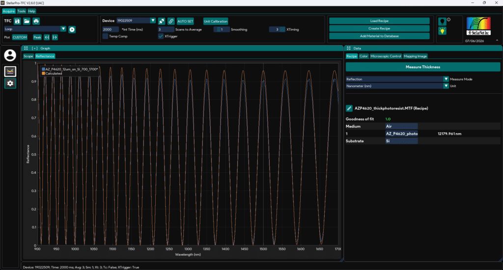
StellarNet Thin Film Measurement System (TF-VIS) measuring thick photoresist used during solar cell manufacturing and photovoltaic process development with optical reflectance spectroscopy.
CdS/CIGS Thin Film Solar Cells
Cadmium Sulfide (CdS) and Copper Indium Gallium Selenide (CIGS) are widely used in high-efficiency thin film photovoltaic devices. The CdS buffer layer forms the p-n junction with the CIGS absorber, while the molybdenum (Mo) back contact provides an efficient electrical interface and influences the optical response of the multilayer structure. Precise measurement of the thickness and optical properties of each layer is critical for maximizing light absorption, charge collection, and overall solar cell efficiency. Spectroscopic reflectometry provides rapid, non-contact characterization of CdS/CIGS/Mo multilayer stacks, enabling researchers and manufacturers to optimize deposition processes, improve device performance, and maintain manufacturing consistency.
Typical Measured Stack
Air
CdS Buffer Layer (40–80 nm)
CIGS Absorber Layer (1–3 µm)
Molybdenum (Mo) Back Contact (~500 nm)
Glass Substrate
Recommended Thin Film System: 350–1700 nm (TF-UVVIS-NIR)
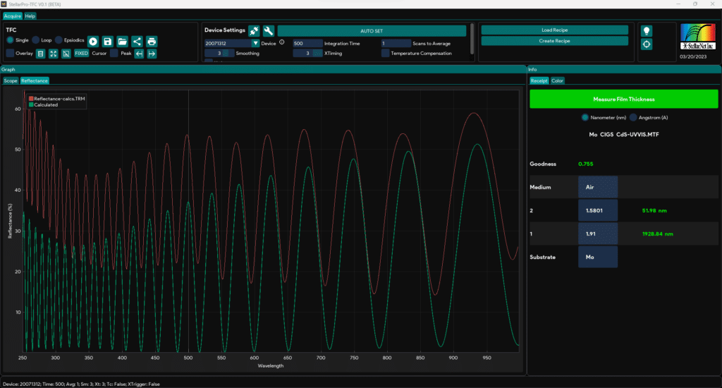
StellarNet Thin Film Measurement System (TF-UVVIS-NIR) analyzing a CdS/CIGS/Mo multilayer photovoltaic structure for film thickness measurement, optical characterization, optical modeling, and CIGS solar cell manufacturing.
Perovskite Solar Cell Multilayer Measurement
Perovskite solar cells consist of multiple functional thin-film layers that work together to achieve high photovoltaic efficiency. Critical layers such as the electron transport layer (TiO₂), perovskite absorber, hole transport layer (Spiro-OMeTAD), and transparent conductive oxide must all be carefully controlled during manufacturing. Spectroscopic reflectometry combined with Transfer Matrix Method (TMM) modeling enables accurate multilayer thickness measurement, providing valuable process feedback for research, pilot production, and next-generation solar cell manufacturing.
Typical Recipe
- Air
- Spiro-OMeTAD (180 nm)
- Perovskite (520 nm)
- TiO₂ (40 nm)
- ITO (150 nm)
- Glass (Bulk)
Recommended Thin Film System: 400–1000 nm (TF-VIS)
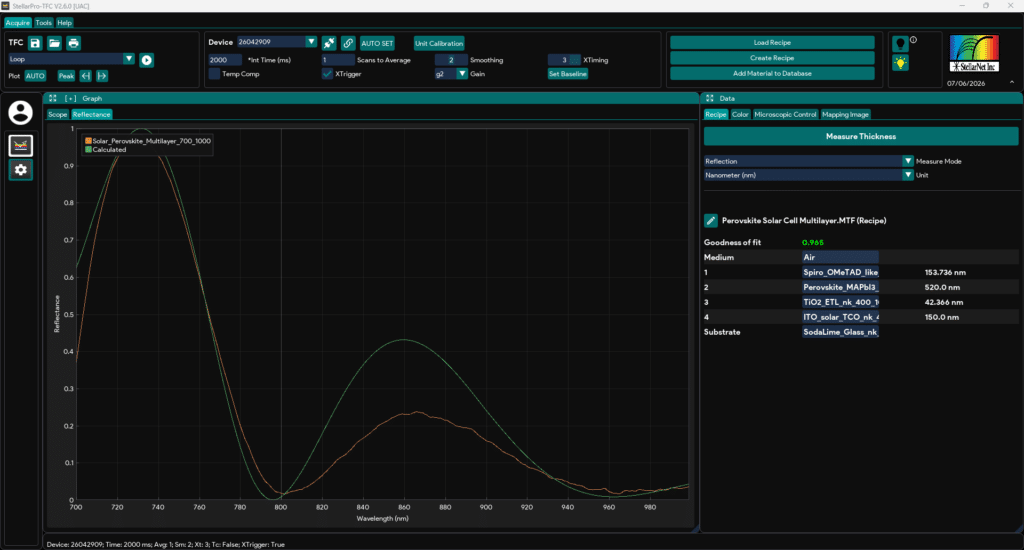
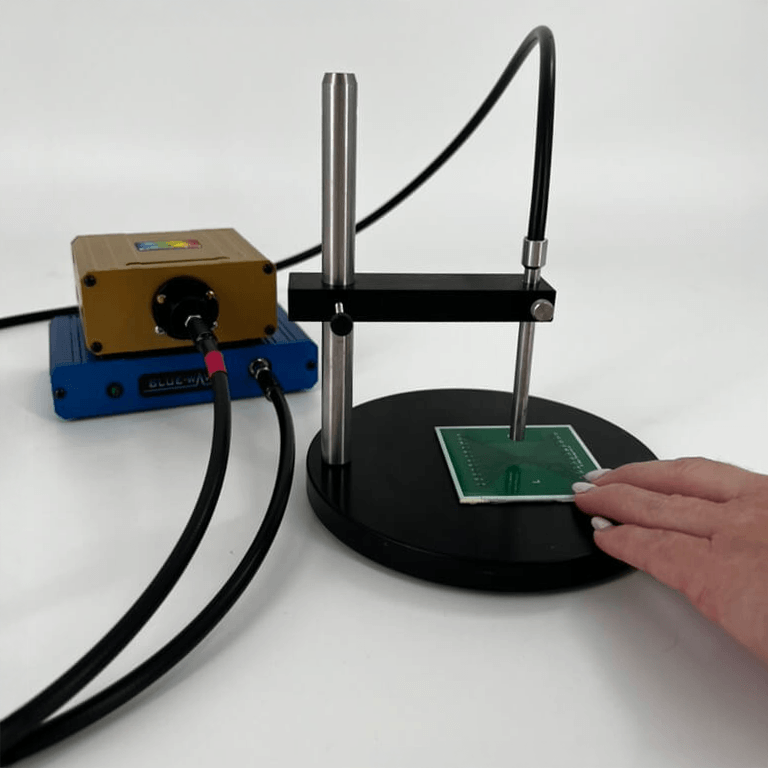
StellarNet Thin Film Measurement System (TF-VIS) measuring a perovskite solar cell multilayer stack using optical reflectance spectroscopy for film thickness measurement, photovoltaic characterization, optical modeling, and solar cell research.
TOPCon Solar Cell Passivated Contact Measurement
Tunnel Oxide Passivated Contact (TOPCon) technology is one of the fastest-growing high-efficiency silicon solar cell architectures. The device consists of an ultra-thin tunnel oxide, doped polysilicon contact layer, silicon nitride anti-reflection coating, and crystalline silicon substrate. Because each layer contributes to carrier transport, passivation, and optical performance, precise thickness control is essential for achieving maximum conversion efficiency. Spectroscopic reflectometry provides rapid, nondestructive characterization of these multilayer structures, making it an effective solution for both research laboratories and large-scale manufacturing environments.
Typical Recipe
- Air
- SiNx (75 nm)
- Poly-Si (160 nm)
- SiO₂ Tunnel Oxide (1.6 nm)
- Crystalline Silicon (Bulk)
Recommended Thin Film System: 500–1700 nm (TF-VIS-NIR)
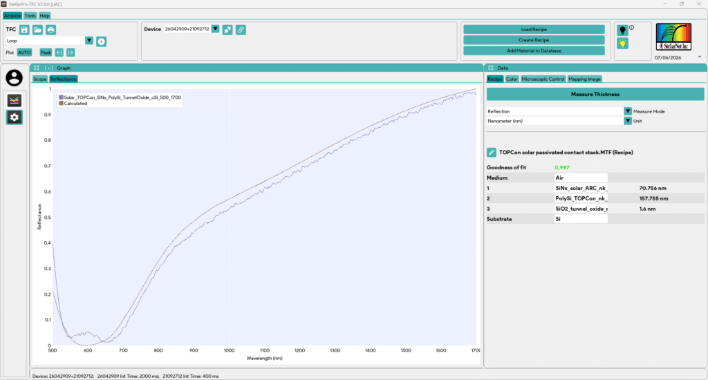
StellarNet Thin Film Measurement System (TF-VIS-NIR) measuring TOPCon solar cell passivation layers using optical reflectance spectroscopy for film thickness measurement, photovoltaic characterization, process monitoring, and solar cell manufacturing.
StellarNet Recommended Thin Film Metrology Systems for Solar & Photovoltaic Applications
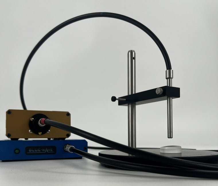
Every solar and photovoltaic application has unique measurement requirements based on material composition, coating structure, device architecture, and performance objectives. StellarNet’s modular thin film metrology platform allows users to configure complete measurement systems using UV-VIS spectrometers, reflectance and transmission fixtures, stabilized light sources, fiber optic probes, and advanced thin film analysis software.
From anti-reflective coatings and transparent conductive oxides to thin film solar cells, perovskite materials, and other photovoltaic coatings, our flexible systems support research, process development, photovoltaic characterization, and production quality control. Our engineer-owned team works directly with customers to configure reliable, non-contact measurement solutions tailored to their solar and photovoltaic applications.
StellarNet TF™ Systems
StellarNet TF™ Systems combine reflectance spectroscopy, precision optics, and intuitive StellarPro™-TFC, Thin-Film Metrology software, to deliver accurate, non-destructive film thickness measurements from approximately 1 nm to 300 µm. The modular architecture allows laboratories to configure the ideal system today while providing a straightforward upgrade path for future automation and advanced measurement capabilities.
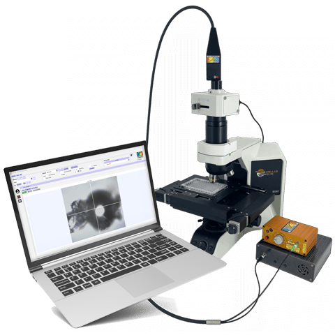
TF-Micro™
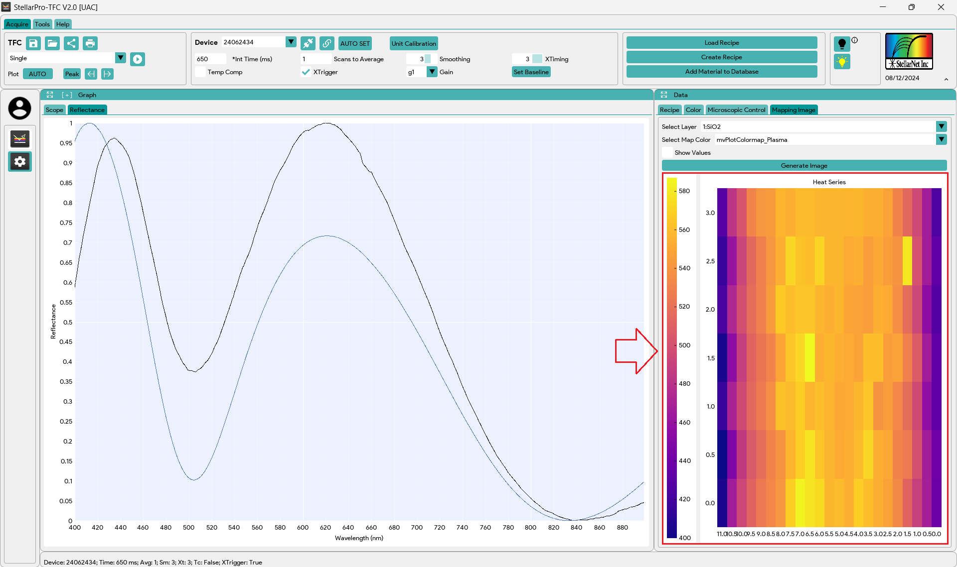
TF-Micro™ upgrades any compatible StellarNet TF™ System with a high-resolution microscope, enabling precision thin-film thickness measurements of microscopic features and small sample areas.
TF-Micro-AM
TF-Micro-AM™ adds programmable XY automation to compatible StellarNet TF™ Systems and TF-Micro™, enabling automated thickness mapping, repeatable positioning, and comprehensive measurement documentation for research and process development applications.
Thin Film Measurement Systems
| System | Range (nm) | Resolution | Thickness | Lamp type | Price |
|---|---|---|---|---|---|
TF-VIS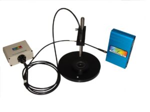 | 400-1000 | <2nm | 10nm-75um | Visible/NIR | $11,500 |
| TF-UVVIS | 200-1100 | <2.5nm | 1nm-75um | UV + Visible/NIR | $14,625 |
| TF-NIR | 900-1700 | <5nm | 100nm-300um | Visible/NIR | $22,655 |
| TF-VIS-NIR | 400-1700 | <2nm, 5nm>1000nm | 10nm-300um | Visible/NIR | $25,280 |
| TF-UVVIS-NIR | 200-1700 | <2nm, 5nm>1000nm | 1nm-300um | UV + Visible/NIR | $28,245 |
| TF-Micro | StellarNet configured Microscope equipped with 4,10, & 40x objectives, CMOS 1.3 Mpixel Camera, optical switch, and required coupling accessories | $11,550.00 |
| TF-Micro-AM | StellarNet configured Auto-Mapping Microscope equipped with 4,10, & 40x objectives, CMOS 1.3 Mpixel Camera, optical switch, and required coupling accessories | $30,975.00 |
Thin Film System Specifications
| Precision | 0.1Å or 0.01% (greater of) |
| Accuracy | 0.2% or 10A (greater of) Film stack dependent |
| Stability | 0.2A or 0.02% (greater of) |
| Spot size | 3mm standard, optional down to 3 µm |
| Sample size | Sample size from 1 mm |
| Computer OS | StellarPro-TFC Software designed for 32 and 64-bit OS |
Technical Information Request
Root zone improvements in spinach through commercial biostimulants application vary among cultivars
Md Noor E Azam Khan, Fahmida Fiza, Joseph G. Masabni, and Genhua Niu | Frontiers in Plant Science | July 13, 2026 | 10.3389/fpls.2026.1830913 Abstract Improvements in root-zone conditions can potentially enhance shoot growth and are especially important in...