StellarNet, Inc. Tampa, Fl USA
10/15/2018
Array Detector Defects and Nonuniformities:
All array detectors, both 1D and 2D, will inevitably suffer from defects and pixel-to-pixel nonuniformities due to the limitations of high-volume semiconductor manufacturing processes. Even in the most tightly controlled semiconductor manufacturing processes, relatively small statistical variations have a large impact resulting in the appearance of dark pixels, hot pixels, and variations in pixel quantum efficiencies, due to the massive numbers of pixels involved. To put this into perspective let’s take a look at the typical scientific imaging camera with a 1024 x 1024 pixel CCD array from Andor Technology (a division of Oxford Instruments) which is specified to have a 0.008% dark pixel rate. While a statistical tolerance of this magnitude is extremely impressive, when you take into consideration that the array contains over 1 million individual pixels, that means that there are over 80 dark pixels which if clustered together can cause dark spots in your image.
When this same analogy is expanded to commercial cameras which can have 20 times the pixel count and far looser tolerancing, it is easy to see how quickly this problem can balloon out of control, making the characterization of imaging arrays a vital step in the quality control process. As a result of these inherent uncertainties, it has become common practice in the detector industry for manufacturers and integrators to measure each array in order to sort and bin them by predetermined performance specifications characteristics. After being sorted into various grades, the resultant detectors can fetch vastly different prices on the market depending on features such as uniformity and hot pixel count.
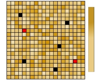
Figure 1 above shows an exaggerated schematic representation of the pixel response is presented for a 20-pixel x 20-pixel array where the black and red pixels represent dark and hot pixels respectively. For lower cost cameras this matrix can be used simply for grading arrays by dark (or hot pixel) density, but in high-end imaging, this mapping of pixel responsivity is used to develop an intensity correction calibration.
Array Detector Testing and Characterization:
In either case, it is imperative to utilize a light source with extremely high spatial uniformity to avoid convolving light source variations with pixel variations. For this purpose here at StellerNet Inc, we have developed the uniform illumination sphere which provides a 2-inch diameter broadband output with an extremely uniform spatial power distribution shown in Figure 2 below. By placing the array at this opening, you are now able to guaranty that each pixel will see the exact same intensity ensuring the accuracy of the measured responsivity matrix.
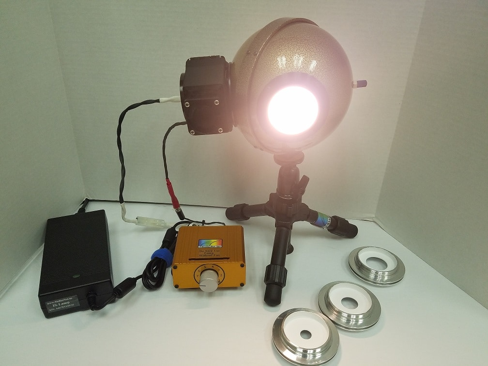
Figure 2: The StellarNet series Uniform Illumination Sphere Light Source and Accessories.
This light source utilizes a 6-inch diameter integrating sphere to homogenize a constant current tungsten or deuterium light source. Integrating spheres are able to accomplish this because the interior of the sphere is coated with a proprietary material which provides diffuse Lambertian reflection with efficiencies greater 99% over the full visible and near infrared spectral range. This diffusely scattered light then bounces around within the integrating sphere creating a uniform “photon cloud” within the sphere, therefore producing a homogeneous power distribution at the aperture.
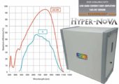
When testing arrays another factor that people often look at is the linearity of the responsivity, which requires that the array is tested at different illumination intensities. But, this variability adds additional complications because the quantum efficiency of the detector is highly dependent of wavelength. By increasing or decreasing the drive current to the lamp will cause the lamp to heat up changing its color temperature and therefore its spectral irradiance. Therefore, we have developed a set of precision drilled aperture plates which can be placed in front of the lamp at the connection to the integrating sphere reducing the intensity without changing the emission spectrum. Figure 3 below shows a comparison of the spectral emission from the same uniform illumination sphere, comparing the difference between these two approaches to varying the lamp intensity.
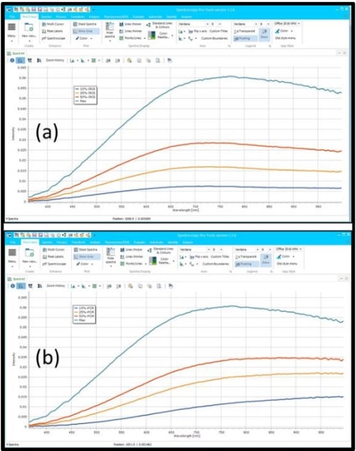
Figure 3: Spectral output of 10W light source with 10%, 25%, 50%, and 100% of max output power utilizing (a)
aperture variation and (b) current tuning.
In Figure 3(a) above you can clearly see that by appertaining the 10W light source the peak wavelength and therefore the correlated color temperature (CCT), of the light source remains constant as the power is adjusted. By contrast in Figure 3(b) where the drive current to the lamp is adjusted the peak wavelength shifts to higher wavelengths which each subsequent decrease in intensity. By analyzing these spectra, it can be shown that at full power the source has a CCT of 3200K, but as the drive current is reduced to 50%, 25%, and 10% the CCT changes to 2900K, 2800k, and 2500k respectively.
Conclusion:
As a result, it is obvious that the uniform illumination sphere light sources by StellerNet provide quality control engineers with an invaluable tool for the test and calibration of both 1D and 2D imaging arrays. This light source is available with StellarNet offers 10, 30, 50, & 75W NIST traceable bulb options depending on your testing requirements and comes with a NIST traceable calibrations certificate and spectral radiance and irradiance data from 300 nm – 1100nm in one-nanometer increments.